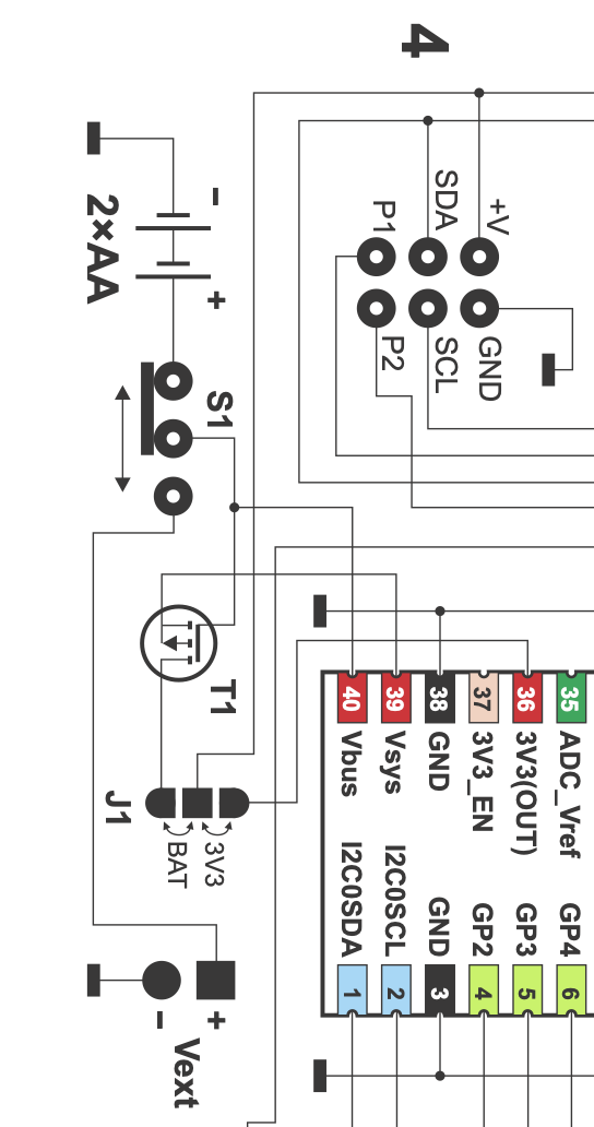
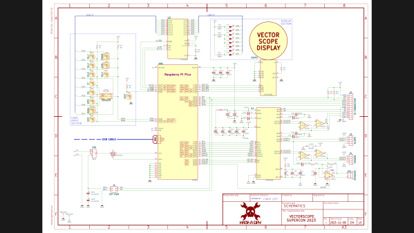
Out of curiosity, I redrew the Supercon Vectorscope badge schematics in KiCad last year. As you might suspect, going from PCB to schematic is opposite to the normal design flow of KiCad and most other PCB design tools. As a result, the schematics and PCB of the Vectorscope project were not really linked. I decided to try it again this year, but with the added goal of making a complete KiCad project. As usual, [Voja] provided a well drawn schematic diagram in PDF and CorelDRAW formats, and a PCB design using Altium’s Circuit Maker format (CSPcbDoc file). And for reference, this year I’m using KiCad v8 versus v7 last year.
Importing into KiCad
This went smoothly. KiCad imports Altium files, as I discovered last year. Converting the graphic lines to traces was easier than before, since the graphical lines are deleted in the conversion process. There was a file organizational quirk, however. I made a new, empty project and imported the Circuit Maker PCB file. It wasn’t obvious at first, but the importing action didn’t make use the new project I had just made. Instead, it created a completely new project in the directory holding the imported Circuit Maker file. This caused a lot of head scratching when I was editing the symbol and footprint library table files, and couldn’t figure out why my edits weren’t being seen by KiCad. I’m not sure what the logic of this is, was an easy fix once you know what’s going on. I simply copied everything from the imported project and pasted it in my new, empty project.
While hardly necessary for this design, you can also import graphics into a KiCad schematic in a similar manner to the PCB editor. First, convert the CorelDRAW file into DXF or SVG — I used InkScape to make an SVG. Next do Import -> Graphics in the Kicad schematic editor. However, you immediately realize that, unlike the PCB editor, the schematic editor doesn’t have any concept of drawing layers. As a work around, you can instead import graphics into a new symbol, and place this symbol on a blank page. I’m not sure how helpful this would be in tracing out schematics in a real world scenario, since I just drew mine from scratch. But it’s worth trying if you have complex schematics.
Note: this didn’t work perfectly, however. For some reason, the text doesn’t survive being imported into KiCad. I attribute this to my poor InkScape skills rather than a shortcoming in KiCad or CorelDRAW. Despite having no text, I put this symbol on its own page in sheet two of the schematic, just for reference to see how it can be done.
Just like last year, the footprints in the Circuit Maker PCB file were imported into KiCad in a seemingly random manner. Some footprints import as expected. Others are imported such that each individual pad is a standalone footprint. This didn’t cause me any problems, since I made all new footprints by modifying standard KiCad ones. But if you wanted to save such a footprint-per-pad part into a single KiCad footprint, it would take a bit more effort to get right.
Recreating Schematics and Parts
After redrawing the schematics, I focused on getting the part footprints sorted out. I did them methodically one by one. The process went as follows for each part:
- Start with the equivalent footprint from a KiCad library
- Duplicate it into a local project library
- Add the text SAO to the footprint name to avoid confusion.
- Position and align the part on the PCB atop the imported footprint
- Note and adjust for any differences — pad size and/or shape, etc.
- Update the part in the project library
- Attach it to the schematic symbols in the usual manner.
- Delete the imported original footprint (can be tricky to select)
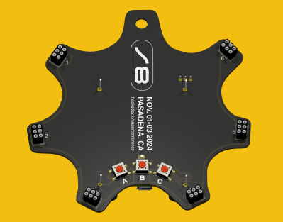
Some parts were more interesting than others. For example, the six SAO connectors are placed at various non-obvious angles around the perimeter. I see that [Voja] slipped up once — the angle between connectors 4 and 5 is at a definitely non-oddball angle of 60 degrees.
SAO Angle Difference
#1   326  102  6->1
#2     8   42  1->2
#3    61   53  2->3
#4   118   57  3->4
#5   178   60  4->5
#6   224   46  5->6
With all this complete, the PCB artwork consists of all new footprints but uses the original traces. I needed to tweak a few traces here and there, but hopefully without detracting too much from [Voja]’s style. Speaking of style, for those interested in giving that free-hand look to hand-routed tracks in KiCad, check the options in the Interactive Router Settings menu. Choose the Highlight collisions / Free angle mode and set the PCB grid to a very small value. Free sketch away.
Glitches
I used two photos of the actual board to check when something wasn’t clear. One such puzzle was the 3-pad SMT solder ball jumper. This was shown on the schematic and on the fully assembled PCB, but it was not in the Circuit Maker design files. I assumed that the schematics and photos were the truth, and the PCB artwork was a previous revision. There is a chance that I got it backwards, but it’s an easy to fix if so. Adding the missing jumper took a bit of guesswork regarding the new and adjusted traces, because they were hard to see and/or underneath parts in the photo. This redrawn design may differ slightly in appearance but not in functionality.
DRC checks took a little more iterating than usual, and at one point I did something to break the edge cuts layer. The irregular features on this PCB didn’t help matters, but I eventually got everything cleaned up.
I had some trouble sometimes assigning nets to the traces. If I was lucky, putting the KiCad footprint on top of the traces assigned them their net names. Other times, I had traces which I had to manually assign to a net. This operation seemed to work sporatically, and I couldn’t figure out why. I was missing a mode that I remember from another decade in a PCB tool, maybe PCAD?, where you would first click on a net. Then you just clicked on any number of other items to stitch them into the net. In KiCad it is not that simple, but understandable given the less-frequent need for this functionality.
You may notice the thru hole leads on the 3D render are way too long. Manufacturers provide 3D files describing the part as they are shipped, which reasonably includes the long leads. They are only trimmed at installation. The virtual technician inside KiCad’s 3D viewer works at inhuman speeds, but has had limited training. She can install or remove all through hold or SMT parts on the board, in the blink of an eye. She can reposition eight lamps and change the background color in mere seconds. These are tasks that would occupy a human technician for hours. But she doesn’t know how to trim the leads off of thru hole parts. Maybe that will come in future versions.
Project Libraries
I like to extract all symbols, part footprints, and 3D files into separate project libraries when the design wraps up. KiCad experts will point out that for several versions now this is not necessary. All (or most) of this information is now stored in the design files, alghouth with one exception — the 3D files. Even so, I still feel safer making these project libraries, probably because I understand the process.
KiCad can now do this with a built-in function. See the Export -> Symbols to New Library and Export -> Footprints to New Library in the schematic and PCB editors, respectively. These actions give you the option to additionally change all references in the design to use this new library. This didn’t work completely for me, for reasons unclear. Eventually I just manually edited the sch and pcb file and fixed the library names with a search and replace operation.
Hint: When configuring project libraries in KiCad, I always give them a nickname that begins with a dot. For example,
.badge24or.stumbler. This always puts project libraries at the top of the long list of libraries, and it makes it easier to do manual search and replaces in the design files if needed.
What about 3D files, you say? That isn’t built into KiCad, but have no fear. [Mitja Nemec] has you covered with the Archive 3D Models KiCad plugin. It was trivial to activate and use in KiCad’s Plugin and Content Manager.
All Done
In the end, the design passed all DRCs, and I could run Update PCB from Schematic... without errors. I went out on a limb and immediately placed an order for five PCBs, hoping I hadn’t overlooked something. But it’s only US$9.00 risk. They are on the way from China as I type this.
All the files can be found in this GitHub repo. If you find any errors, raise an issue there. I have not done this procedure for any of the SAO petals, but when I do, I will place a link in the repository.


